
As semiconductor fabs become increasingly power intensive under the demands of AI workloads, advanced lithography systems, and 24-hour production cycles, manufacturers are turning to industrial IoT and predictive analytics to reduce energy consumption without compromising uptime.
According to Jérôme Tourdiat of Schneider Electric, the next phase of energy optimisation inside semiconductor manufacturing will depend less on standalone hardware upgrades and more on connected electrical infrastructure capable of generating large volumes of operational data.
Speaking to Automation News, Tourdiat said Schneider Electric’s EcoStruxure platform is already helping semiconductor manufacturers reduce energy consumption by up to 20% through predictive maintenance and AI-driven operational optimisation.
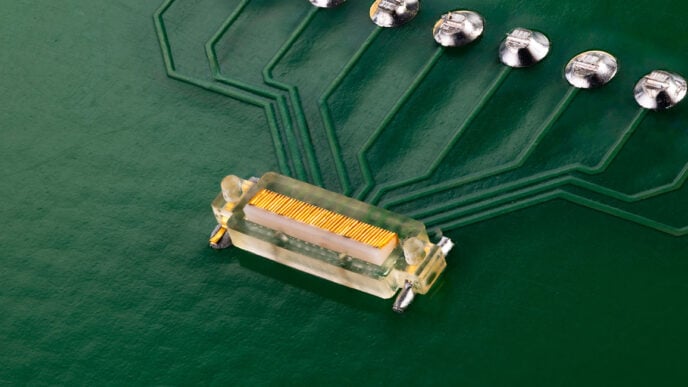
At the core of the system is an extensive network of industrial IoT sensors embedded throughout a fab’s electrical distribution infrastructure.
Multiple sensors
“In each critical point within the medium-voltage and low-voltage equipment — especially around busways and important electrical connections — we install sensors that monitor different conditions,” Tourdiat said.
The company typically deploys multiple sensors inside medium-voltage switchgear cabinets throughout a semiconductor site. Depending on the scale of the facility, a fab may contain anything from a handful of cubicles to more than 100 distributed across the plant.
These sensors continuously monitor operating conditions such as temperature, humidity, insulation degradation, electrical load behaviour, and partial discharge activity. The resulting data streams are consolidated into Schneider’s software platform, where machine learning models analyse the information to identify inefficiencies or detect signs of impending failure before equipment breaks down.
“The quality of the data is key for AI,” Tourdiat said. “The more data you have, the better trained the AI becomes, and the more benefit customers can get from the system.”

One of the most important technologies within the system is partial discharge monitoring. Partial discharge refers to small electrical sparks or insulation failures that occur before a larger electrical breakdown develops. These early-stage faults can generate subtle thermal or electrical anomalies long before operators would traditionally identify a problem.
“If you can detect those early warning signs, you can intervene before the equipment overheats or breaks down,” Tourdiat said.
For semiconductor manufacturers, the commercial impact of these systems is closely tied to uptime. Any unplanned interruption inside a fab can have major consequences for production schedules, equipment utilisation, and yield.
Tourdiat said predictive maintenance systems can reduce downtime by between 15% and 30%, while also lowering unnecessary maintenance activity by allowing operators to intervene only when equipment condition data indicates a developing issue.
The company claims one semiconductor deployment achieved a six-month return on investment alongside annual energy savings of approximately 18,000 megawatt hours, although Schneider Electric declined to identify the customer involved.
When asked whether the use of AI itself risked offsetting some of the energy savings, given the growing power demands associated with large AI models and data centres, Tourdiat argues that industrial AI models are significantly less power hungry and that the additional computing demand was far outweighed by the resulting efficiency gains.
“These models are not large language models,” he said. “They are much smaller models that can run on premises. They do not consume so much energy as the large models used for video or generative AI.”
A major challenge for the sector, however, is that many semiconductor facilities still operate large amounts of legacy infrastructure that was never designed to be digitally connected.
Legacy systems offer opportunities
“The legacy systems are probably where we can optimise most,” Tourdiat said. “But it is not always easy to access the data, because much of the equipment was installed before connectivity was considered.”
As a result, many energy optimisation projects now involve retrofitting electrical infrastructure with new sensing and monitoring systems capable of generating the data needed for predictive analytics.
By contrast, newer fabs are increasingly designed around connected electrical architectures from the outset.
Beyond the fab floor itself, Schneider is also integrating microgrid technology into semiconductor energy management strategies. These systems allow operators to balance electricity from the grid with on-site renewable generation and battery storage systems in order to reduce both energy costs and carbon emissions.
Tourdiat said similar technologies are increasingly being deployed inside hyperscale data centres, where AI-driven computing demand is pushing electrical infrastructure towards significantly higher power densities.
The company is also exploring wider use of direct current power architectures to reduce conversion losses in high-density computing environments, although semiconductor fabs remain primarily alternating current-based for now.
“It is still early days,” Tourdiat said. “But moving towards DC is probably one of the solutions to reduce losses and therefore reduce consumption.”